Soft materials are all around us and play a significant role in our everyday lives. They include materials such as synthetic polymers, biopolymers, liquid crystals, colloids and nanoparticles, animal and plant cells are found in many foods, personal care products, clothing, medicines, paints and inks and biological tissues to name but a few examples. Soft materials display a rich physics that is not usually observed in simple liquids and crystalline solids and we routinely exploit the properties of these materials. A relatively simple example of this can be found in toothpaste which is designed to flow during application but to resist flow once applied to the toothbrush. This so called "shear thinning" behaviour is a common property of many soft material systems.
A particularly striking property of many of these systems is the viscoelastic nature of their mechanical response. When deformed on short timescales these materials behave like elastic solids and on longer time scales they exhibit flow characteristics that are more like a viscous liquid. This particular effect is due to the fact that the relaxation times of the component parts of these systems are comparable to experimentally accessible timescales. These materials have such interesting properties because their constituent parts have structural elements that have dimensions which lie somewhere between the atomic length scale (10-10 metres) and macroscopic length scales (1 millimetres). For example, polymers contain long chain molecules that can be tens of nanometres in size and colloids contain small particles that can be anywhere from five nanometres to one micron in diameter.
At Nottingham we have a range of different active research projects in soft materials physics. These include (but are not limited) to studies of:
We have a good balance of ongoing pure and applied research in these areas and we welcome applications from any new students wishing to do a PhD in our group.
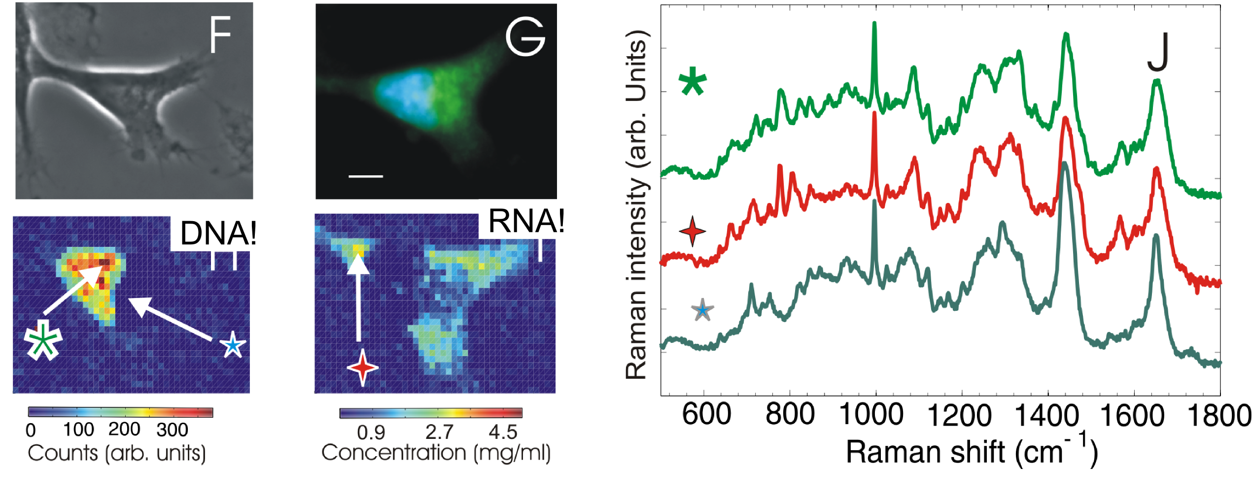
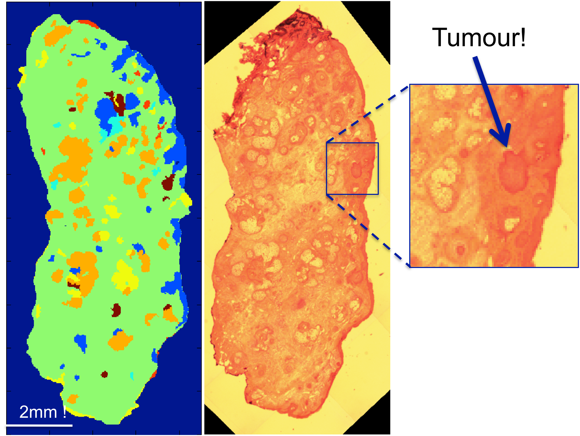
Optics and spectroscopy have the potential to underpin fundamental advances in our understanding of molecular and cellular processes. This potential may be realised in nanoscale studies of single molecules, through the mesoscale of individual live cells up to the macroscale of in-vivo disease diagnosis and imaging. Recent developments in laser and light detection technology allow imaging of biological materials with unprecedented detail. In particular, imaging techniques based on molecular spectroscopy can detect small chemical alterations in cells and tissue with sub-micron scale resolution, providing insight into cellular processes and allowing label-free diagnosis of diseases.
At Nottingham we have a range of different active research projects. These include (but are not limited) to:
We have a good balance of ongoing pure and applied research in these areas and we welcome applications from any new students wishing to do a PhD in our group.
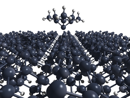
We investigate the organisation of complex molecules on surfaces with the aim of understanding how large scale structures are determined by local intermolecular interactions such as hydrogen bonding, halogen bonding and metal-co-ordination. These studies include the spontaneous formation of open nanoporous molecular networks which can be used as nanoscale containers to capture other materials and control growth on a surface. In addition we have recently identified an arrangement stabilised by hydrogen bonding where entropy plays a significant role and we are planning future studies to extend this approach to other disordered molecular tilings to investigate exotic two-dimensional phases and quasi-crystalline ordering. Collaborations with Nottingham chemists (Champness) form an important part of this activity.
The packing of macromolecules on surfaces has emerged as an important current theme and these materials display novel structural properties due to the competition of their interactions and internal elastic deformation. These studies have included linear porphyrin polymers with interesting optoelectronic applications and we are now focussing on analogue nanorings – cyclic structures formed as closed loop polymers. This worked is performed in collaboration with chemists at Oxford (Anderson).
The growth of one- and two-dimensional polymers on surface is being investigated in the group as a route to form graphene analogue materials. Several coupling reactions are being investigated as routes to extended two-dimensional networks which have a high degree of connectivity across macroscopic areas. We have also developed methods to release these films from the substrates on which they are formed using a molecular adhesive (based on fullerene thin films) and are now exploring the optical and electronic properties of the resulting materials.
We are also developing techniques to fabricate double layer graphene devices in which a thin layer of material is sandwiched between two graphene electrodes. The ‘sandwich’ layer is chosen to be insulating and must be very thin, down to a few nanometres. We are currently exploring organic materials for tunnel barriers, biomolecular nanosheets for dielectrics, colloidal quantum dots, layered optical emissive materials and metal-organic frameworks (see below).
Metal-organic frameworks are ordered crystalline materials in which organic molecules (often linear) form connections through metal ions. This results in a material in which molecular rods are connected by metal ions to form a highly open porous structure. These materials are of great interest for the capture and storage of gases as well as sensors and for catalysis. In collaboration with Nottingham chemists Champness and Schroder we have started a new programme to grow this films of metal organic frameworks which is aimed both at technological applications and a fundamental study of the initial phases of growth.
We would be very interested to hear from prospective PhD students who are interested in the following projects:
A major research theme within the Nanoscience Group is the exploitation of dynamic force microscopy for the imaging, spectroscopy, and manipulation of individual atoms and molecules. Dynamic force microscopy is an exceptionally powerful technique which exploits shifts in the resonant frequency of a vibrating cantilever to map the variation in the interaction between a sharp tip (at the end of the cantilever) and an underlying sample. If that tip is atomically sharp then not only is it possible to image individual atoms but the force between two atoms can be mapped out with resolution on length scales comparable to the width of individual electron orbitals. Or, as shown by Gross and co-workers at IBM Zurich, the 'architecture' of a single molecule can be imaged with unprecedented resolution. Even more excitingly, single atoms and molecules can be manipulated one at a time purely through mechanical force.
Our force microscopy - and, more generally, scanning probe microscopy - research falls into three broad categories, which we outline below. The Nanoscience Group currently coordinates the multi-partner ACRITAS European training network. ACRITAS focuses on actuation and characterisation at the single bond limit using different types of atomic force microscopy. All of our force microscopy work relies on strong collaborations with a variety of groups both here at Nottingham (including those of Janette Dunn, Physics and Astronomy; Neil Champness, Chemistry; and Natalio Krasnogor, Computer Science, in the UK, and internationally. An especially important collaboration in recent years has been our joint projects with Lev Kantorovich and co-workers at King's College London.
Our research in this area can be broadly categorised into three different sections:
An exciting and rapidly evolving sub-field of nanoscientific research is the use of dynamic force microscopy to manipulate atoms through (chemo)mechanical force alone. A number of groups worldwide, including a number of members of the ACRITAS network, have made pioneering in-roads in this direction. Our focus in Nottingham is on the manipulation of atoms at silicon surfaces using the qPlus technique pioneered by Franz Giessibl.
The video below describes the trials and tribulations associated with our initial experiments in this field. Our aim is now to extend this type of approach to a broader range of Group XIV elements (Ge, Sn, Pb) on the Si(100) surface in order to build three-dimensional nanostructures, atom-by-atom and under computer control.
Transferring a single molecule from a surface onto a force microscope tip can not only facilitate extremely high resolution imaging (as shown by Leo Gross and co-workers at IBM Zurich, it also enables the measurement of intermolecular force-fields and potential energy landscapes. We have recently carried out the first direct measurement of the intermolecular potential for two C60 molecules using this strategy. Atomic resolution force microscopy of the fullerene cage adsorbed on the force microscope tip (using the electron orbitals of the underlying surface as a 'probe') enabled us to determine the orientation of the C60 molecule. This ability to modify molecular orientation with atomic precision has particular potential in the measurement of the force-fields for more complex molecules (hydrogen-bonding species, porpyhrins, phthalocyanines, etc…) and this will form the basis of our future work in this area.
Images obtained using scanning probe microscopies are usually explained with the aid of density functional theory (DFT) calculations. In our case, we collaborate closely with Lev Kantorovich on DFT calculations. DFT can be very time-consuming, however, especially when a functionalised tip is used to image complex molecules. Janette Dunn's group is developing computationally-fast methods of interpreting STM and AFM images based on Hückel and extended Hückel methods. These are not ab initio methods so can't be used as predictive tools. However, they provide very fast means of simulating images for a given situation. This approach has been used to interpret experimental images of C60 fullerene molecules on Si surfaces. It has been particularly successful at explaining images obtained using a C60-functionalised tip to image C60 surface molecules. Simulated images for given orientations of the tip and sample molecules can be obtained in a matter of minutes on a desktop computer. The orientations that provide the best matches to experimental images agree with those postulated theoretically elsewhere.
Ultrahigh vacuum (UHV) scanning probe microscopy enables arguably the ultimate control of condensed matter (via single atom manipulation/positioning) and has been associated with some of the most exciting, inspirational, and elegant experimental work in condensed matter science. Unfortunately, it can also be one of the more frustrating techniques used in experimental science, with many fruitless hours spent on attempting to coerce the probe into a structure that yields, retains, and accurately reproduces atomic resolution images. Collectively, vast numbers of researcher person-months in the scanning probe and nanoscience research communities are therefore currently wasted in conditioning STM and AFM tips (during the scanning process) via voltage pulsing, field emission, high bandwidth scanning, high (or low) feedback loop gains, and other "tricks of the trade".
We are developing, through a joint Physics - Computer Science collaborative approach, a "one click" set of algorithms and protocols which will instead automate the optimisation of tip structure (and tip chemistry), representing a radical, and dramatically more efficient, departure from conventional working methods in scanning probe experimentation. The video below shows the automatic optimisation of an STM tip to provide atomic resolution of the Si(111)-(7x7) surface, involving no human operator involvement (other than moving the tip to the sample surface). The first ten seconds of the video show the tip being driven into a graphite surface in order to provide a stringent test for the software.
The key researchers involved in the automated optimisation project are Richard Woolley and Julian Stirling. An open-source toolbox for advanced processing of scanning probe microscopy images, stemming from the automated optimisation project, is now available from http://julianstirling.co.uk/software/spiw/.
Over the last decade our group has been working towards extending electrospray ionization to the deposition of large and fragile molecules on surfaces under ultra-high vacuum conditions (UHV) for investigation using synchrotron-based electron spectroscopy and scanning probe microscopy. Why? Because oftentimes we want to deposit complex molecules on surfaces with intrinsic functionality, but the complexity that gives rise to this functionality often makes the molecules too fragile to be thermally evaporated. Electrospray deposition overcomes this problem by taking the molecules directly from solution and producing a molecular beam that can be used to deposit these molecules on surfaces at pressures compatible with UHV techniques. With electrospray deposition we are fast approaching a situation in which we can deposit virtually any molecule on any surface.
The technique works by passing a solution of the molecules through a narrow capillary tube held at a very high voltage. The electric field causes the ions to be drawn towards a counter electrode until the force is so great that the surface tension is overcome and a jet of charged droplets emerges. These droplets undergo a series of explosion events because they hold too much charge for their surface tension to hold them together, and a fine plume of charged solvated molecules is formed. This plume is extracted into vacuum and skimmed by a series of differentially pumped apertures until we have a beam of molecules that can be directed to impinge on our surface held in ultra-high vacuum.
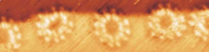
UHV-ESD has enabled us to study organometallic dye molecules adsorbed on titanium dioxide surfaces using advanced synchrotron radiation-based electron spectroscopy to measure the charge transfer dynamics at the heart of dye-sensitised solar cells and to verify the chemical synthesis of giant porphyrin nanorings by imaging them on a surface using STM. We have even managed to deposit the highly fragile Mn12-based single molecule magnets onto a gold surface and verify the presence of an intact magnetic core (see image to the right) and continue to work on innovative solutions to desolvation, soft-landing and energy selection of the deposited molecules. Our work in UHV-ESD is also supported by Molecularspray Ltd through an industrial CASE studentship.
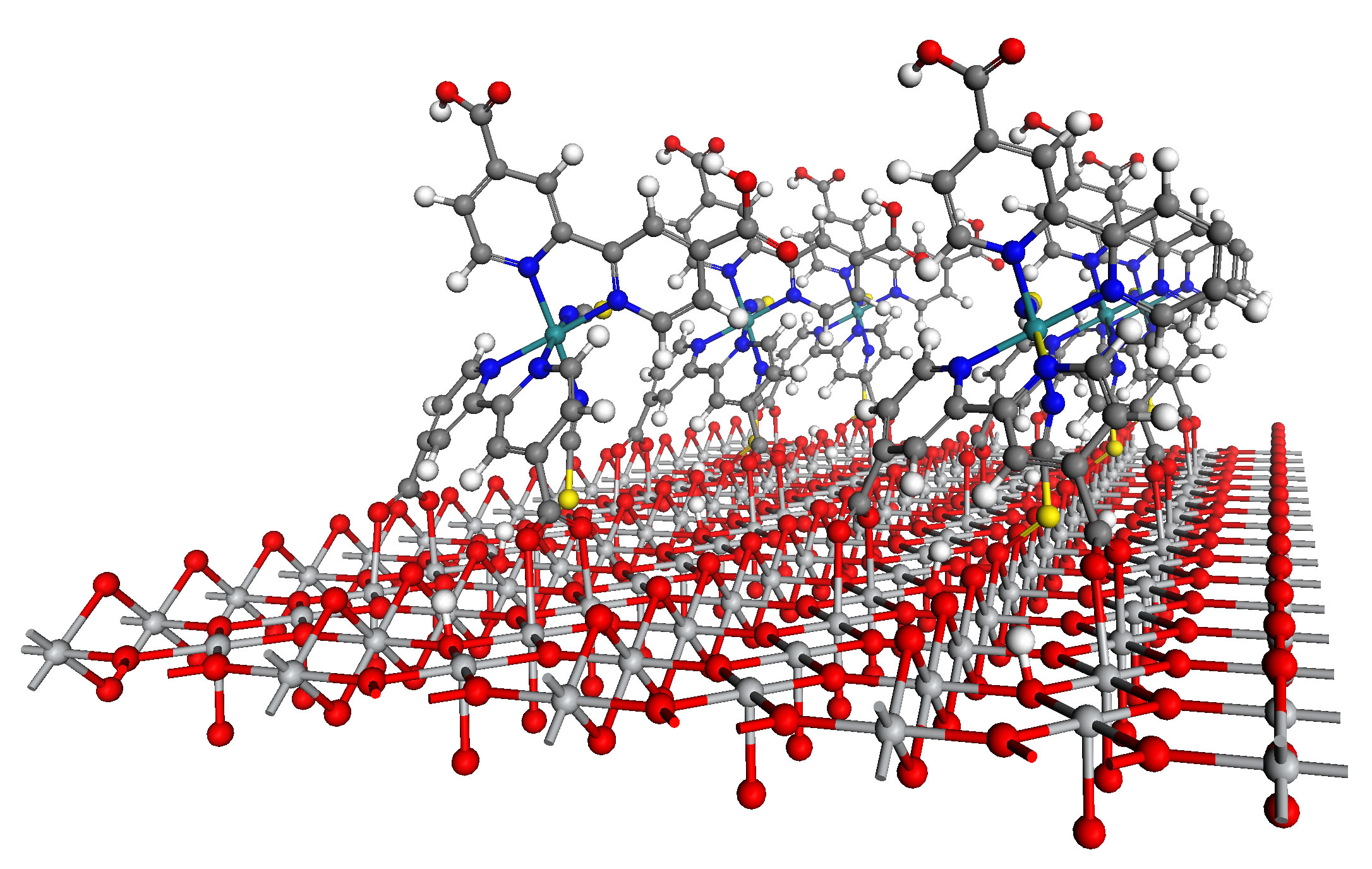
Charge transfer between a molecule and a solid surface lies at the heart of a number of really important devices such as solar cells and organic LEDs. To make a dye-sensitised solar cell for example you can take TiO2 which doesn't absorb visible light (this is evident by the fact that it's white) and coat it with a single layer of dye molecules similar to those shown in the figure to the right. The dye can absorb a photon of visible light, exciting an electron into a previously unoccupied molecular orbital, which can then tunnel into the conduction band of the oxide to which it is bound. Not only does this provide electrons in the conduction band, but the electron and hole are immediately separated.
Clearly, the interaction of the dye molecule with the oxide surface is key to our understanding of the underlying physics. We use a variety of synchrotron radiation techniques (at MAXlab in Sweden and SOLEIL in France), including photoemission (PES) and X-ray absorption spectroscopy (XAS) to investigate the chemical nature of the adsorbed molecules and their bonding geometry. Going beyond this, using the 'core-hole clock' implementation of resonant photoemission (RPES) we can actually measure how quickly an electron tunnels from the molecule to the substrate on the timescale of the lifetime of core-hole, on the order of a few femtoseconds.
Basically, when a core-electron is excited into a previously unoccupied molecular orbital it leaves the atom in a core-excited state. This state is unstable and will decay on the timescale of femtoseconds. The mechanism by which it decays can either be radiative (it releases a photon) or non-radiative (it releases an electron) as depicted in the figure to the right. In the case of non-radiative decay, a valence electron falls down to fill the core-hole and sufficient energy is given to another valence electron so that it can escape the atom. We can tell whether the originally excited electron was involved in this process by measuring the kinetic energy of all the electrons that are emitted, and infer from this how long the excited electron remained on the molecule before tunnelling into the conduction band of the oxide surface.
Using this technique we have measured the charge transfer dynamics of a range of complex molecules on titanium dioxide related to dye-sensitised solar cells and water splitting devices (see publications). In the case of radiative decay, a soft x-ray photon is emitted from the atom. Measuring the energy of this photon is not so easy and the numbers of photons emitted from the carbon and nitrogen atoms that we are interested in have a very low abundance. However, using a technique known as resonant inelastic x-ray scattering (RIXS) we can measure the energy of the emitted photons and compare the number emitted at the same energy as the incoming photon (elastic scattering) to those at a lower energy (inelastic scattering).
In another beautifully complicated scheme this information can also tell us how long the originally excited electron remained on the molecule before tunnelling, and so this technique is a complementary method to RPES for measuring ultra-fast charge transfer dynamics in adsorbed molecules. Its advantage is that it is a photons-in-photons-out technique and can therefore be applied to buried interfaces and high-pressure systems. We have recently provided the first experimental evidence for this method from our work at MAXlab, and continue to develop this technique at SOLEIL.
Applying these techniques to study the complex molecules used in real solar cells and water splitting devices requires a method to controllably deposit them onto a surface under the UHV conditions required by the relevant spectroscopic techniques. To this end we have been developing a portable system (as shown in figure to the right) for in-situ UHV-compatible electrospray deposition (see Complex Molecules at Surfaces) at synchrotron beamlines and other UHV systems.